(China (Mainland))

Product Summary
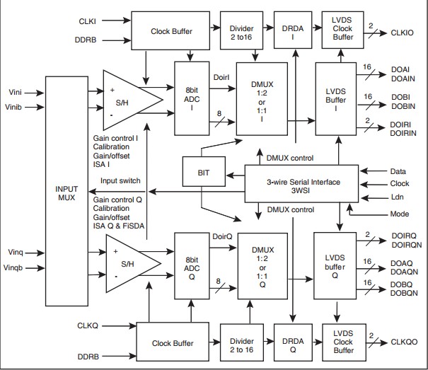
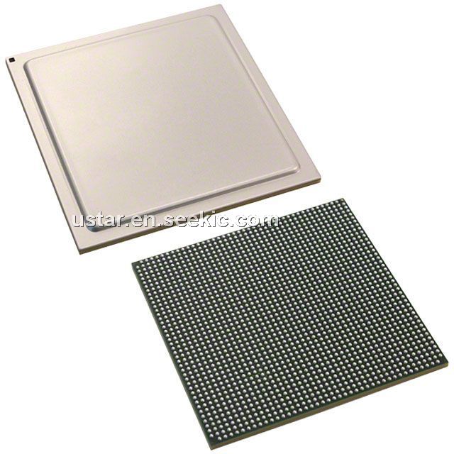
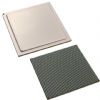
The AT84AD001BVEPW is a monolithic dual 8-bit analog-to-digital converter, offering low 1.4W power consumption and excellent digitizing accuracy. The AT84AD001BVEPW integrates dual on-chip track/holds that provide an enhanced dynamic performance with a sampling rate of up to 1 Gsps and an input frequency bandwidth of over 1.5 GHz. The dual concept, the integrated demultiplexer and the easy interleaving mode make this device user-friendly for all dual channel applications, such as direct RF conversion or data acquisition. The smart function of the 3-wire serial interface eliminates the need for external components, which are usually necessary for gain and offset tuning and setting of other parameters, leading to space and power reduction as well as system flexibility. The applications of the AT84AD001BVEPW include Instrumentation, Satellite Receivers, Direct RF Down Conversion, WLAN.
Parametrics
AT84AD001BVEPW absolute maximum ratings: (1)Analog positive supply voltage VCCA: 3.6 V; (2)Digital positive supply voltage VCCD: 3.6 V; (3)Output supply voltage VCCO: 3.6 V; (4)Maximum difference between VCCA and VCCD VCCA to VCCD: ± 0.8V; (5)Minimum VCCO VCCO: 1.6 V; (6)Analog input voltage VINI or VINIB VINQ or VINQB: 1/-1 V; (7)Digital input voltage VD: -0.3 to VCCD + 0.3 V; (8)Clock input voltage VCLK or VCLKB: -0.3 to VCCD + 0.3 V; (9)Maximum difference between VCLK and VCLKB VCLK - VCLKB: -2 to 2 V; (10)Maximum junction temperature TJ: 125℃; (11)Storage temperature Tstg: -65 to 150℃; (12)Lead temperature (soldering 10s) Tleads: 300℃.
Features
AT84AD001BVEPW features: (1)Dual ADC with 8-bit Resolution; (2)1 Gsps Sampling Rate per Channel, 2 Gsps in Interlaced Mode; (3)Single or 1:2 Demultiplexed Output; (4)LVDS Output Format (100?); (5)500 mVpp Analog Input (Differential Only); (6)Differential or Single-ended 50? PECL/LVDS Compatible Clock Inputs; (7)Power Supply: 3.3V (Analog), 3.3V (Digital), 2.25V (Output); (8)LQFP144 Package; (9)3-wire Serial Interface.
Diagrams